
3D simulations using software
We covered 2D simulations in our previous discussion on 2D thin film calculations. Here we will introduce the software techniques which are employed to find the reflection, transmission, and phase from 3D objects, and to optimize the resonances produced by the said objects. We will only discuss one software, namely Lumerical FDTD solutions, which employ the finite difference time domain (FDTD) method. We will be making the same two-layer thin film multilayer design (discussed in the previous discussion) in this software and simulate the design for the optical and near-infrared regimes (350-1050 nm).
Simulation example in Lumerical FDTD solutions
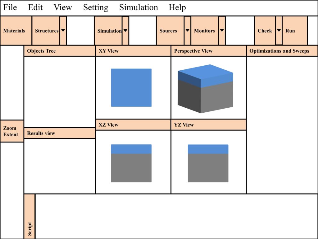
When Lumerical FDTD solutions software is opened, we can see a blank page with four views of x-y, perspective view, x-z, and y-z. The main menu has File, Edit, View, Simulation, and Help submenus. There is a toolbar of different operations underneath it, from which important tools, needed for simulation, will be discussed later on. Then beneath these toolbars, on left we have an object tree and on the extreme right, we have optimization and sweep tree. The steps taken to simulate a multilayer bi-layer thin film of 150 nm chromium (Cr) layer beneath a 50 nm silicon dioxide (SiO2) layer are as follows.
Complete simulation tutorial
The major elements which will be used in this tutorial of running simulations in Lumerical FDTD solutions are shown in Fig. 1.
- When you open the software you need to first set the dimensions from Setting>Length Units>Nanometer (since we are simulating for the optical regime, nanometer dimension is more convenient).
- Then we need to set the time units to femtoseconds from Setting>Time units>Femtosecond (also because we are simulating in optical regime).
- Now open “Materials” (tool found beneath the main menu) for curve fitting. Then press “go to material explorer” when the menu of “Materials” opens. Select “Cr-Palik” from the menu found beneath “Material setting” Set the min wavelength on right (underneath simulation bandwidth settings) to 350 (if it is in nm, otherwise set it to 0.35 if the length is in μm) and set the maximum wavelength to 1050 (if it is in nm, otherwise set it to 1.05 if the length is in μm). Now on the right side of these settings, set the vertical axis to the refractive index to view the curve fitting of the refractive index. Now press “fit and plot” on the lower right side of the window. Check whether the line passes through the points data points and if it does, check the curve fitting for SiO2-Palik in the same manner for the same wavelength range. The line for SiO2 should pass through the center as SiO2 is not dispersive in optical and near-infrared regimes. So refractive index of SiO2 should just be a line at around 1.46. The Cr is dispersive and if the curve of the FDTD model does not pass through its data points the fit tolerance and max coefficients should be changed unless the model curve fits data points.
- When satisfied curve fitting is attained close the Materials window and save setting to apply simulation bandwidth.
- Now add structures by Structures toolbar on the right side of Materials. Select rectangle from the drop-down ↓ menu on Structures. Now rectangle could be seen on the object tree. Right-click on the rectangle and press edit object. Change the name of the rectangle to Cr layer. In geometry set the x-span, and y-span to 300 nm. Set the z-min to -150, and z-max to 0.
- Now press the Material tab on the edit rectangle window. Select the Cr-Palik from the drop-down material menu and press ok.
- Similarly, add another rectangle, having the same x-span and y-span, but this time change its z-min to 0 and z-max to 50 and change its name to SiO2 layer. In the materials tab, select SiO2-Palik from the drop-down material menu and press ok.
- Now in the toolbar below the main menu, find the “Simulation” toolbar. Press its drop-down menu and select region. This region will show as FDTD in the object tree. This tool defines the region or space for which the simulation will take place. Only the objects inside this region will be the active structures that take part in changing the reflection, transmission, or absorption.
- Now right-click on FDTD and press edit object. Select geometry from the menu of the edit object window. Set x-span and y-span as 200, and set z-min as -400 and z-max as 550. These values of z-min and z-max can be changed to reduce simulation requirements, which will be discussed later in this post.
- Now go to Mesh settings from the menu of the edit object window. There are different types of mesh type. The default mesh type will be auto non-uniform with a mesh accuracy of 2. Usually, mesh accuracy can be increased to increase the mesh (a grid for which electromagnetic wave equations are calculated to generate a final response). In auto non-uniform does automatic meshing and it is closely spaced in regions where the boundary of materials is present. A uniform mesh type can also be selected where mesh steps can be defined. We will perform this simulation with auto non-uniform mesh type and with mesh accuracy of 3.
- Now go to Boundary conditions from the menu of the edit object window. Select periodic for x min bc, x max bc, y min bc, y max bc, and select the perfectly matched layer (PML) for z min bc and z max bc. The periodic means that we have set our object to be repeated periodically in x and y planes, but not in z plane. This scheme considers the object present inside the region to be infinitely present in x and y dimensions. Press ok and exit the edit object window of FDTD.
- Now select FDTD in the object tree and press zoon extent from the view toolbar (can also be selected from view in the main menu), which will zoom the entire FDTD block in the view area.
- Click on the drop-down menu of the Sources tool present on the right of the Simulation, and underneath the main menu and select the Plane wave. This plane wave will appear on the object tree as the source. Select source from objects tree and press Edit object. Select the Direction source to be Backward. Select the Geometry tab from the edit object window and set x-span and y-span to 200 and set z to be 400 (this represents the place where the source will be placed). Select the Frequency/Wavelength tab from the edit object window and observe whether wavelength start and wavelength stop are 350 and 1050, respectively. Press Ok to exit window.
- Click on the drop-down menu of the Monitors tool present on the right of the sources, and underneath the main menu and select the Frequency-domain field and power. This step will add a monitor in the objects tree. Select monitor and press Edit object. Change the name of the monitor to Reflection. In the General menu, tick override global settings, tick use linear wavelength spacing, and set frequency points to be 351. In the Geometry menu of the edit object window of the monitor, set x-span and y-span as 200, and set z to be 500 nm. Press Ok to exit window.
- Click on the drop-down menu of the Monitors tool present on the right of the sources, and underneath the main menu and select the Frequency-domain field and power. This step will add another monitor in the objects tree. Select monitor and press Edit object. Change the name of the monitor to Transmission. In the General menu, tick override global settings, tick use linear wavelength spacing, and set frequency points to be 351. In the Geometry menu of the edit object window of the monitor, set x-span and y-span as 200, and set z to be -300 nm. Press Ok to exit window.
- Now click on the drop-down menu of the Check tool present on the right of the Monitors to see whether the simulation requirements do not exceed your computer’s RAM and hard drive. If the instructions are properly followed until here, all of the requirements will be below 100 mb for this example simulation tutorial. Press Ok to exit window. Press Run on the right side of the check tool and save your simulation file (if not saved already).
- Wait for the simulation to complete.
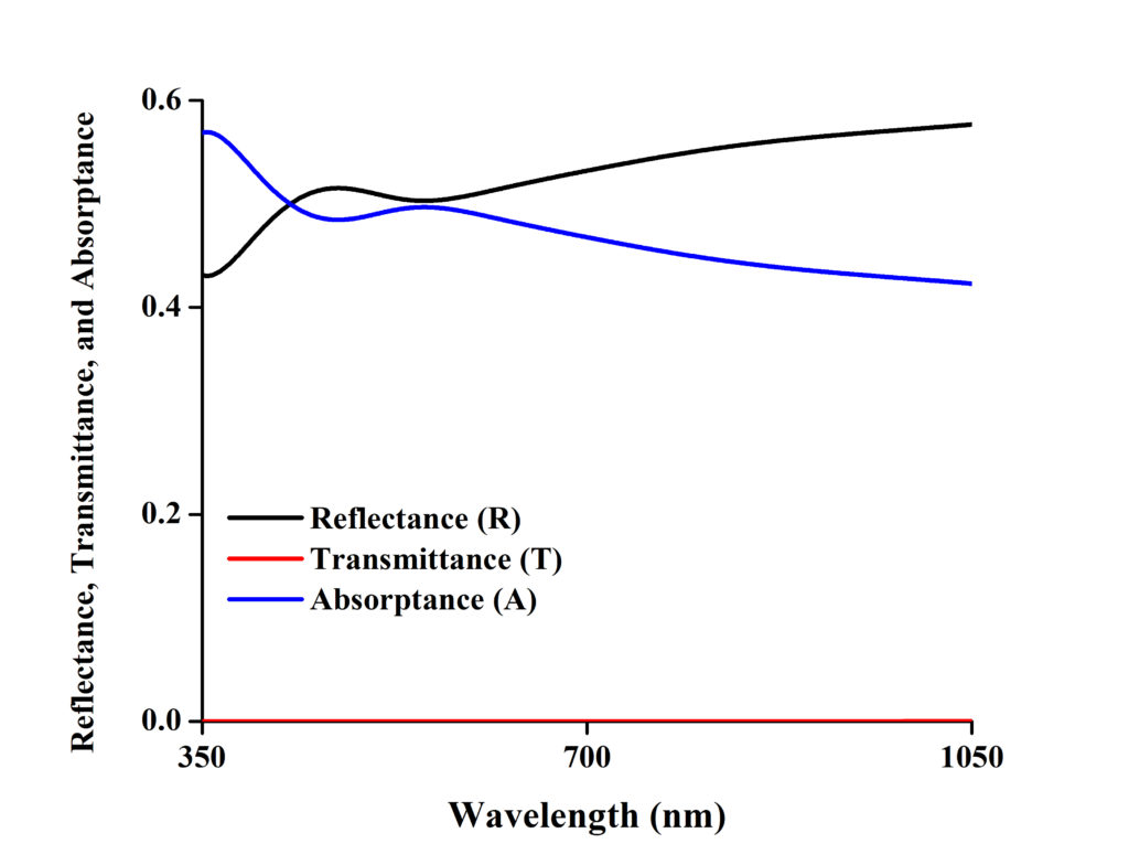
- Right-click on Reflection monitor, hover over visualize, and select T from the drop-down menu. This step will plot the reflectance from our design. Export the results by pressing export and clicking clipboard in the drop-down menu to copy the 351 data points with values of reflection at equidistant wavelengths. This can be copied to the clipboard or MS excel. Press Ok to exit the window.
- Right-click on Transmission monitor, hover over visualize, and select T from the drop-down menu. This step will plot the transmittance from our design. Select the scalar operation to be abs to convert negative values of transmission to positive. Export the results by pressing export and clicking clipboard in the drop-down menu to copy the 351 data points with values of reflection at equidistant wavelengths. This can be copied to the clipboard or MS excel. Press Ok to exit the window.
- Verify the results from the following image (Fig. 2) showing reflection, transmission, and absorptance (obtained by subtracting reflectance and transmittance from 1).
Similarly, complex 3D objects can be simulated in this environment and same methods can be applied to obtain results.